Skip to content
Setcoin Group
CRITICAL INFRASTRUCTURE • SUPPLY CHAIN SOVEREIGNTY

DSE Semiconductors Manufacturing Fund

Strategically deploying capital into advanced semiconductor fabrication facilities, critical equipment and materials supply chains, and next-generation packaging and testing infrastructure. The fund targets the most critical chokepoints in the global semiconductor value chain — where capacity constraints meet unprecedented demand from AI, automotive electrification, and edge computing.

Fund type: EquityStatus: Actively Investing

Setcoin Atlas · live pipeline

The pipeline behind the fund

What the public record shows today in the sectors DSE Semiconductors Manufacturing Fund invests in. The fund screens from the same Atlas records, and every project is scored on the Bankability Index.

65projects in play: pre-FID with at least one consent gate on the public record10 verified at shovel-ready or later after an in-depth screen
76projects in development (pre-FID)
$203.1bnpre-FID capex (filed or modeled)
102already under construction

By stage (Bankability Index)

  • No gate yet11
  • Award / offtake only58
  • Pre-consent7
  • Shovel-ready0
  • Bankable0

Highlighted rows are in play. Few projects reach shovel-ready or bankable on public evidence alone, because EPC and offtake contracts are rarely published; a Screen on the dataroom moves them. Bars on a square-root scale.

By region

  • United States63
  • Europe & UK11
  • Asia-Pacific2

Verified shortlist: screened in depth, names withheld

#RegionWorking stageReadinessCapexGates on the record
1United States · ArizonaFID70$100.0bnlandconsentpermitsgridofftakeepcsponsorcapital
2United States · TexasFID56$15.0bnlandconsentpermitsgridofftakeepcsponsorcapital
3United States · New YorkFID56$11.6bnlandconsentpermitsgridofftakeepcsponsorcapital
4CzechiaFID55$1.8bnlandconsentpermitsgridofftakeepcsponsorcapital
5GermanyFID55$240mlandconsentpermitsgridofftakeepcsponsorcapital
6United States · GeorgiaBankability59$340mlandconsentpermitsgridofftakeepcsponsorcapital
7United States · TexasBankability59$25.0bnlandconsentpermitsgridofftakeepcsponsorcapital
8United States · ArizonaBankability59$5.0bnlandconsentpermitsgridofftakeepcsponsorcapital
9United States · MichiganShovel-ready52$770mlandconsentpermitsgridofftakeepcsponsorcapital
10IndiaShovel-ready26$340mlandconsentpermitsgridofftakeepcsponsorcapital

Source: Setcoin Atlas — interconnection queues, permit and state registers, award databases. Figures update with each Atlas build. Named projects, sponsors and evidence are available to registered investors in the LP workspace.

Dual-Track Model

The Fund is Currently Raising & Actively Investing

Whether you're an institutional investor seeking exposure to the semiconductor manufacturing buildout, or a company seeking growth capital for fab construction, equipment production, or packaging capacity, we want to hear from you.

For Ventures & Projects

Submit Your Project

We are actively seeking semiconductor manufacturing, equipment, packaging, and materials ventures at FEED and FID stages. If you have a project addressing critical supply chain gaps with proven technology, we want to hear from you.

  • Capital at critical development stages
  • Late-stage, expansion, and project financing
  • Additional offtaking demand from portfolio company ecosystem
  • Partnerships across the semiconductors value chain
  • Strategic support for government subsidy applications
  • Strategic support for government procurement

For Investors

Invest in the Fund

Join leading institutional investors gaining exposure to the most critical infrastructure buildout of the decade — semiconductor manufacturing capacity that underpins AI, electrification, and national security.

  • Institutional-grade semiconductors infrastructure exposure
  • Access to high-return semiconductor infrastructure investments
  • Diversified across fabs, packaging, equipment, and materials
  • Government-subsidised projects (CHIPS Act, EU Chips Act)
  • Faster ROI than leading-edge fabs via enabling technologies
  • Co-investment opportunities on select deals

Investment Strategy

Targeting the Chokepoints That Control $1 Trillion

The DSE Semiconductors Manufacturing Fund capitalises on a structural shift: the primary bottleneck in semiconductors has moved from leading-edge lithography to advanced packaging, high-bandwidth memory, and compound semiconductor manufacturing. The highest-ROI opportunities now lie in these enabling technologies — requiring 1/5th the capital of leading-edge logic fabs, with faster time-to-revenue and lower geopolitical risk. By focusing on FEED and FID-stage projects benefiting from government incentive programs, the fund aims to de-risk investments while capturing outsized returns from capacity-constrained markets.

  • Wafer fabrication cleanroom with automated tools

    Advanced Fabrication Facilities

    Leading-edge logic (2nm/1.4nm) and memory chip fabs, mature node capacity (28nm–180nm) for automotive and industrial, and specialty semiconductor manufacturing plants.

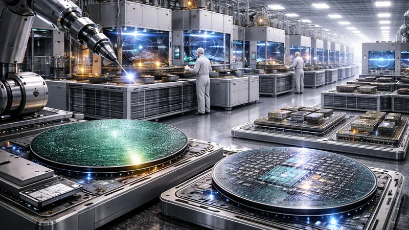
  • Robotic arm handling advanced packaging substrates in a cleanroom

    Advanced Packaging & Testing

    CoWoS and 2.5D/3D packaging capacity, HBM manufacturing expansion, chiplet ecosystem infrastructure, and automated test equipment providers.

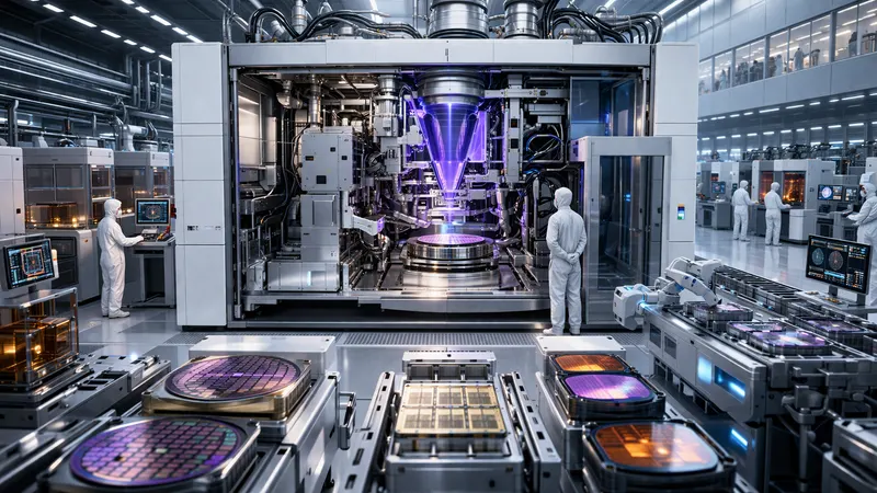
  • Lithography and deposition equipment on a semiconductor production floor

    Equipment & Tooling

    Lithography, etching, and deposition equipment. ALD tools, high-productivity etch systems, advanced metrology and inspection equipment for next-generation nodes.

  • Ultra-pure chemical and specialty gas handling for semiconductor manufacturing

    Materials & Chemicals

    EUV photoresists, ultra-pure neon and specialty gases, ABF substrate alternatives, silicon wafer capacity, and advanced thermal interface materials.

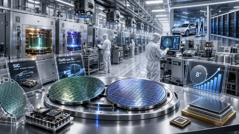
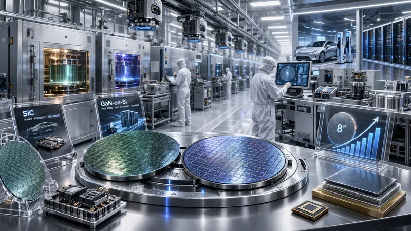
  • Silicon carbide wafers being processed on a compound semiconductor line

    Compound Semiconductors

    SiC substrate and device manufacturing for automotive EV inverters. GaN-on-Si device fabrication for datacenter power and fast charging. 8-inch wafer transition acceleration.

  • Automated wafer logistics inside a semiconductor supply chain facility

    Supply Chain Security

    Western photoresist manufacturing for geopolitical hedging. Substrate material diversification. Neon recycling systems. PFAS-alternative development for plasma etching.

Geographic Focus:

  • United States
  • European Union
  • United Kingdom
  • Japan
  • Australia
  • Middle East
  • India
  • Vietnam

Infrastructure Investment Priorities

Infrastructure Priority Matrix

The fund deploys capital across three tiers based on criticality, time-to-revenue, and return potential. Tier 1 priorities control the most acute chokepoints in AI and automotive supply chains.

TIER 1 — CRITICAL

Build Immediately

12-24 month deployment windows

InfrastructureTimelineMarket Impact

Advanced Packaging Capacity (CoWoS)

12-18 mo

TSMC's CoWoS capacity is critically short — AI accelerator demand alone requires 3x current capacity. Building 15–20K wafer/month CoWoS-equivalent facilities, independent of leading-edge fabs, offers the fastest ROI in semiconductors.

3–4 Year Payback

HBM Manufacturing Expansion

24-30 mo

High-Bandwidth Memory supply is 40% short of demand with only 3 global suppliers. Dedicated HBM manufacturing lines (not converted DRAM capacity) targeting HBM3E today and HBM4 by 2027.

4–5 Year Payback

SiC Substrate & Device Manufacturing

18-24 mo

SiC power device market growing at 38% CAGR. Current capacity covers only a fraction of 2030 demand. Targeting 300K+ 8-inch equivalent wafers/year for EV inverters, charging, and grid storage.

3–4 Year Payback
TIER 2 — HIGH PRIORITY

Strategic Capacity Expansion

18-36 month deployment windows

InfrastructureTimelineMarket Impact

Mature Node Fabs (28nm–65nm)

18-24 mo

Critically short for automotive MCUs, power management, RF, and analog. Targeting 60–80K wafers/month in cost-advantaged regions with government partnership essential for economics.

6–8 Year Payback

GaN-on-Si Device Fabrication

24-36 mo

Leveraging existing 150nm–250nm silicon fabs for 48V datacenter power, fast charging, and RF applications. Lower capex than greenfield SiC with proven existing infrastructure.

3–4 Year Payback

Western Photoresist Manufacturing

24-36 mo

Strategic supply chain security imperative for U.S. and EU fabs. Currently dominated by Japanese suppliers with China restriction risk. EUV, ArFi, and KrF photoresist production.

7–10 Year Payback
TIER 3 — STRATEGIC R&D

Next-Generation Technologies

24-60 month deployment windows

InfrastructureTimelineMarket Impact

Alternative Patterning Technologies

36-48 mo

Directed Self-Assembly (DSA) for sub-3nm nodes and nanoimprint lithography for memory. Pilot line investment to position for post-EUV manufacturing paradigms.

R&D Pilot Lines

Heterogeneous Integration R&D Centers

30-36 mo

Chiplet design and validation infrastructure. UCIe (Universal Chiplet Interconnect Express) ecosystem development. Co-located with major design hubs.

Ecosystem Play

Advanced Metrology & Inspection

36-60 mo

High-NA EUV actinic inspection, in-line AI-driven defect detection, and sub-nanometer overlay metrology. KLA alternative development opportunity.

Monopoly Disruption
  • TIER 1 — CRITICAL

    3 priority targets

    12-24 month windows

  • TIER 2 — HIGH PRIORITY

    3 priority targets

    18-36 month windows

  • TIER 3 — MEDIUM PRIORITY

    3 priority targets

    24-60 month windows

Supply Chain Intelligence

Critical Bottlenecks We're Targeting

The fund thesis is built on deep analysis of the semiconductor supply chain's most constrained nodes — where demand visibility is highest and supply gaps create outsized return opportunities.

  • Critical Constraint

    Advanced Packaging Capacity Gap

    AI accelerator demand requires 40–50K CoWoS wafers/month by 2026 — current capacity is ~15K. Samsung and Intel are 18–24 months behind TSMC. Through-Silicon Via manufacturing yields and thermal management in 3D stacks remain key technical challenges.

  • High Constraint

    EUV Lithography Equipment Monopoly

    ASML is the sole supplier of EUV systems with 18–24 month lead times. High-NA EUV systems cost $350M each. Downstream chokepoints exist in EUV photoresist (only 3 qualified suppliers) and photomask manufacturing.

  • Structural Gap

    Mature Node Capacity Shortage

    28nm–180nm capacity critically short for automotive and industrial. New construction is economically unattractive at low ASPs. Legacy equipment manufacturers exiting mature node tools, constraining the refurbished equipment market.

  • Critical Constraint

    HBM Supply Crisis

    Only 3 suppliers globally (SK Hynix 60% share, Samsung, Micron). HBM3/HBM3E supply 40% short of demand. HBM4 requires 1,000+ TSV connections per die stack with multiplicative yield loss across 12–16 layer configurations.

  • High Constraint

    Compound Semiconductor Capacity (SiC, GaN)

    SiC power device demand outpacing supply by 3–5 years. Current capacity ~300K 6-inch wafers/year versus 2–3M wafer equivalents needed by 2030. The 8-inch transition is happening too slowly with substrate yields below 50%.

  • Structural Gap

    Critical Materials & Single-Source Risks

    ABF substrate monopoly (Ajinomoto), neon gas concentration, ultra-pure photoresist chemicals dominated by Japanese suppliers, and PFAS environmental regulations limiting fluoropolymer production for plasma etching.

What We're Looking For

Investment Criteria for Projects

We actively seek semiconductor manufacturing, equipment, and materials ventures that address critical supply chain gaps and demonstrate strong technology readiness.

  • FEED/FID Stage Readiness

    Projects nearing Final Investment Decision with completed feasibility studies, EPC quotations, equipment procurement plans, and detailed project schedules.

  • Government Incentive Alignment

    Projects benefiting from CHIPS Act, EU Chips Act, or equivalent national programs. Subsidies essential for mature node economics and strategic supply chain security.

  • Proven Process Technology

    Companies with cutting-edge or proven process technologies, strong IP portfolios, and demonstrated manufacturing yield track records. TRL 7+ for core processes.

  • Critical Supply Chain Position

    Facilities and technologies addressing verified supply chain gaps — monopoly disruption, single-source risk mitigation, and capacity-constrained market segments.

  • Secured Offtake & Demand Visibility

    Long-term offtake agreements or binding customer commitments. Preference for projects with locked-in demand from hyperscalers, automotive OEMs, or government contracts.

  • Experienced Operational Team

    Ventures led by teams with deep semiconductor manufacturing experience, process engineering expertise, and track records in fab ramp-up and yield optimisation.

Geographic Focus:

  • United States
  • European Union
  • United Kingdom
  • Japan
  • Australia
  • Middle East
  • India
  • Vietnam

Value Creation Strategy

Beyond Capital: Strategic Value-Add

  • Fab Ramp Acceleration

    Technical expertise to accelerate time-to-production and yield learning curves.

  • Supply Chain Integration

    Connecting portfolio companies across the semiconductor value chain.

  • Subsidy Navigation

    Expert support for CHIPS Act, EU Chips Act, and national incentive applications.

  • Market Intelligence

    Setcoin Intelligence research on demand trends, pricing, and competitive dynamics.

  • Geopolitical Advisory

    Export control compliance, dual-use technology assessment, and risk mitigation.

Risk Management

Comprehensive Risk Mitigation

The fund employs rigorous due diligence and risk management across technical, market, geopolitical, and financial dimensions.

  • Yield & Technical Risk

    Staged funding tied to yield milestones; KGD testing protocols; redundancy in design.

  • Equipment Availability

    Early commitment programs, alternative vendor development, equipment-sharing agreements.

  • Talent Shortage

    University partnerships, training programs, immigration policy coordination.

  • Market Cyclicality

    Long-term offtake agreements, countercyclical capacity additions, portfolio diversification.

  • Geopolitical & Export Control

    Geographic diversification, dual-sourcing, ITAR/EAR compliance frameworks.

  • Capital Intensity

    Government subsidies, JV structures, asset-light models where viable.

Related Intelligence

Frequently Asked Questions

Fund Questions, Answered

What is the DSE Semiconductors Manufacturing Fund?

A Luxembourg-domiciled equity fund managed by Setcoin Group that invests in advanced semiconductor fabrication, critical equipment and materials supply chains, and next-generation packaging and testing infrastructure.

Which semiconductor chokepoints does the fund target first?

Tier 1 (12-24 month deployment windows) covers advanced packaging capacity (CoWoS, €4-6B), HBM manufacturing expansion (€10-15B) and SiC substrate and device manufacturing (€2-3B) — the constraints where AI accelerator and EV demand most exceeds supply.

What kind of projects and companies can apply?

Semiconductor manufacturing, equipment, packaging and materials ventures at FEED and FID stage with proven process technology (TRL 7+), secured offtake or demand visibility, alignment with CHIPS Act or EU Chips Act incentives, and experienced fab ramp-up teams.

Why enabling technologies rather than leading-edge fabs?

The fund's thesis is that the primary bottleneck has moved from leading-edge lithography to advanced packaging, high-bandwidth memory and compound semiconductors. These require roughly 1/5th the capital of leading-edge logic fabs, with faster time-to-revenue and lower geopolitical risk.

Who can invest?

Qualified institutional investors only — pension funds, sovereign wealth funds, endowments, family offices, insurers, corporates and funds of funds. Terms are set out in the fund's Private Placement Memorandum.

Where does the fund invest?

United States, European Union, United Kingdom, Japan, Australia, Middle East, India and Vietnam.

How to Start

Ready to Capitalise on the Backbone of AI Economy?

Whether you're looking to invest in the fund or submit a semiconductor manufacturing project for funding consideration, we're ready to start the conversation.

Investor Access Request

Request Access to DSE Semiconductors Manufacturing Fund

Request access to participate in the fund targeting critical semiconductors infrastructure bottlenecks

Luxembourg
Domicile
Actively Investing
Status

Contact Information

Organization Details

Investment Interest

Anticipated commitment

Additional Information

Compliance & Consent

Important Disclosure

This form is for informational purposes and does not constitute an offer to sell or solicitation of an offer to buy any securities. Investment in the DSE Semiconductors Manufacturing Fund is available only to qualified investors and involves significant risks including potential loss of principal. Past performance is not indicative of future results. All investments are subject to the terms and conditions set forth in the fund's Private Placement Memorandum (PPM).

Venture & Project Submission

Submit Your Semiconductors Manufacturing Opportunity

We are actively seeking semiconductor manufacturing ventures and infrastructure projects addressing critical supply chain bottlenecks. Tell us about your project.

What are you submitting?

Contact Information

Project Overview

Project Stage & Timeline

Current Project Stage

Project Sector

Project Financials

Total Project Cost

Data Room Documentation

Required Documentation for FEED / FID Projects

The following documentation demonstrates project shovel-readiness and enables thorough evaluation with reduced risk and uncertainty. Please confirm availability and provide data room access below.

Documents available in your data room
Risk Assessments: The level of detail and comprehensiveness of your project manual is crucial—it demonstrates shovel-readiness and enables prospective investors and lenders to thoroughly evaluate the opportunity with reduced risk and uncertainty.

Secure link to your existing data room (Intralinks, Datasite, Google Drive, etc.)

PDF or PowerPoint, max 25MB

Submission Consent

Confidentiality Assurance: All submissions are treated as strictly confidential. Your information will only be shared with our investment team for evaluation purposes. We do not share deal flow with portfolio companies or other investors without explicit consent.